Super Class D UcD2000 Fullbridge Tips - PCB Layout PDF
Hello guys, in this post I will give tips, test points, settings, and troubleshooting on the UcD2000 Fullbridge class-D amplifier whose PCB layout can be downloaded at the end of the post for single-layer PCB, for PCB Layout version of Gerber files can be downloaded in the following post: UcD2000 Fullbridge
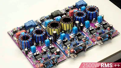
And I designed the UcD2000 Fullbridge PCB Layout myself, so I know exactly how the paths and component placements are. The PCB Layout that I share is fixed for the path and component values listed on the PCB.
PCB with a double-layer path can be printed on JLCPCB. you can print it on JLCPCB with the downloaded Gerber file. Why should you be in JLCPCB? Because the JLCPCB is fast, the price is cheap, the quality of the PCB is very good, the delivery is also fast, it can ship all over the world.
First, visit the JLCPCB site. then log in or register first (if you don't have an account) the button is in the top right corner. If you have logged into your account, then just click "Order Now"
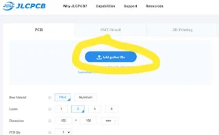
Then click "Add Gerber file"
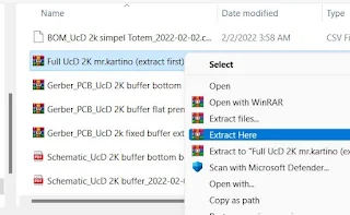
Select the Gerber file that has been downloaded at the end of the post link, but before using the downloaded file, the file with the name "Full UcD 2K mr.kartino (extract first)" must be extracted first.The file already contains schematic same as PCB marking, BoM files, and PCB Layout gerber, for Gerber there are three, 1 for amplifier board, and 2 buffer versions.
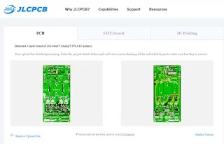
Then select Gerber one by one, then double click. Wait for the upload process to complete.
Then select Gerber one by one, then double click. Wait for the upload process to complete. then if you want to add another Gerber file, just click "Add Gerber file" again. if the three PCBs have been uploaded and have selected the option for each PCB, then click the basket, and just go to payment by clicking (Secure Checkout), and complete the payment on the next page. Payment can use a credit card, or debit visa, and also PayPal.
The UcD Fullbridge PCB has been fixed, I have tested it myself and the results are very satisfying, the PCB just needs to be installed according to the label listed on the PCB, you can be sure it works as long as the components are not installed correctly, and the soldering is good. What I often encounter is failure in assembling the UcD2000 or class-D amplifier which is purely my design, usually the wrong component is installed, or the value is not correct on the PCB, for example a 1nF capacitor, the writing is correct on the 1nF component but after measuring it with the Avometer, it turns out that the value is far off the mark. listed. so do resistors, usually poor quality capacitors or resistors can be like that. Therefore, why is this amplifier trying to use good components, it's not just class-D that is trying to use good or quality components, actually all Amplifier classes are the same as trying to use good components so that the results are maximum, for example resistors at least using thick-legged resistors and does not stick to the magnet.
Before assembling the amplifier, prepare the components first
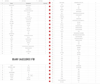
following BoM or component list UcD2000
Resistors that are not called watts use a 1/4W. Resistor
Elco which is not called voltage can use a minimum of 16V
For R Shunt R28 R2 R1 R70 , use a good 3W resistor. and it's better if each component leg is given a heatshrik, so it's safer, (for example, when it's on, you want to plug the speaker terminal instead of hitting the leg of the R shunt resistor which can eventually kill the zener) so it's better if the R shunt leg is wrapped.
Zener 5V can use zener 5V1 D21 D8
Zener 12V D39 D40 can use zener 12V-15V
Other Zeners must be the same as PCBs
R Gate 22R 1/2 W if you can use 0.5W if you use 1/4W use a good resistor.
Settings
The R marked with 2 stars "PCB" can also be used for gain settings, a smaller value means the gain will increase, and vice versa.
R with 1 star can also be used for setting gain, but it also causes the speed pwm value to change, the value of R is getting bigger, the gain is also increasing.
For speed settings, it can also be from 1 star R, R30 R71, the higher the speed, the higher the pwm speed, it can also be from capacitors C22, C37, C28.
R Slope Balance, R45, The larger the resistor value, the wider the side min (left) and side + (right) are getting narrower, the indication of the mosfet or ir can be (the hotter the narrower) it can be played R 45 In this case, if R45 is getting smaller then the opposite, the right IR section is getting wider, the left IR is getting narrower.
Download the PDF layout for easy component identification once the part is plugged in:
Download Top Layer PCB: Top Layer UcD2000 Fullbridge v2.3
Download Bottom Layer PCB: Bottom Layer UcD2000 Fullbridge v2.3
Schematic Amplifier: UcD2000 Fullbridge v2.3
Video Assembling
Do you have diagram d3k9 130vdc?
ReplyDelete