Booster Amplifier circuit ( Transistor Final )
The circuit of booster amplifiers or amplifier end of a power amplifier circuit, Circuit over in the most important influence whether or not , and many more are affected in this final amplifier circuit.
Booster Amplifier Circuit Diagram :
Because the booster circuit is the amplifier end of the work was too heavy components causing the rapid component of the heat. If you are wrong when install the components, that can cause fatal damaged the component , such us the installation of pin emiter, collector , and base everything must be correct.
In the circuit above can strengthen booster amplifier with maximum work and everything is evenly split, what is it evenly split ? evenly split the point here is that all components can work with the same voltage and the heat evenly , this is because at each respetive base transistor were given the same constrains and same wattage resistor. And to maintain if the power output is too large then the resistor on Re will hamper so that the transistor is not easily broken.
Part List Booster Amplifier / Final Transistor :
Re=0,5-1R/5W
Q1=Transistor power NPN such us 2N3055 , TIP3055,TIP120,TIP142,2SC2922 , 2SC5200 , etc.
Q2=Transistor Power PNP such us MJ2955 ,TIP2955,TIP125,TIP147,2SA1216, 2SA1943 , etc.
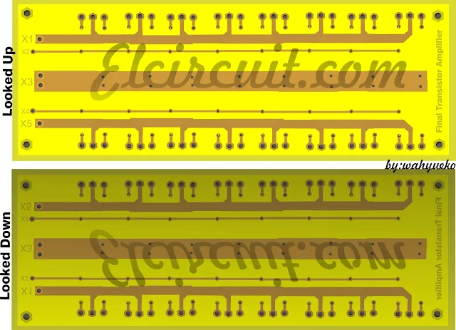
X1=Voltage connector (-)
X2=PNP Base connector
X3=Speaker connecor but also must be connected from the buffer
X4=NPN base connector
X5=Voltage connector (+)
 |
| 2SC5200 2SA1943 Ex Transistor Final |
PCB Layout Booster amplifier ( Transistor Final )
 |
For power amplifier driver you can search here: Power Amplifier Circuit [VIDEO] See Also Assembling Final Transistor Amplifier |


I LIKE THIS...?
ReplyDeletethanks sir
DeleteThis comment has been removed by the author.
ReplyDeleteFor driver you can using this power amp circuit :
Delete2800W High Power Amplifier Circuit
Thanks sir! Perfect layout schematic diagram very nice!
ReplyDeleteHello jhun,
DeleteThanks for your visit and hope you enjoy surfing in here. in elcircuit dot com.
how many volts DC minimum and maximum for this booster amplifier
ReplyDeleteHello henry,
DeleteIts same as voltage power amplifier. For example you make 1600W the power supply voltage from 60 up to 100V dc, so the voltage of booster tramsistor is sam 60 upto 100V DC.
Thanks Henry,
HOPE YOU ENJOY in elcircuit.
THANK YOU VERY MUCH FOR THE INFORMATION,
ReplyDeleteThanks Mr.Wahyu
Hello Henry,
DeleteYoure welcome, dont be hesitate to ask with me, may i can help you.
Thanks
Connect must by like this? (Or in place TIP36C-TIP35C?)
ReplyDeletehttps://drive.google.com/file/d/0B7s82YdStJGRQWk3bnZJZWxXVlU/view?usp=sharing
u must replace the tip35c tip36c, and connet x4 to emitter bd139 and x2 to emitter bd140
ReplyDeleteThanks for fast reply!!
Deleteu're wellcome, Hope u enjoy in here sir.
Deletevc tem o pdf completo
ReplyDeletenice design,,, but where can i input and its output for speaker,, is it ok to have no driver/?
ReplyDeleteoutput ke bad ka cirki dalo thanku
ReplyDeletePa approved po
ReplyDeletei will make this if someone is gonna sale me a parts...nice schem
ReplyDeletegood morning, how many millivolts should the bias trimmer be calibrated? And the second trimmer? Sincerely Marcuzzi Rudi.
ReplyDeleteLa resistenza R8 è da 3k3 oppure 33k ? Il progetto cosa richiede ?
ReplyDelete