
Exploring PCB Surface Finish A Comprehensive Guide
The PCB surface treatment process is a crucial step in PCB manufacturing. Its purpose is to protect the copper surface from oxidation and ensure that it can bond well with the solder during the soldering process. The following are some common PCB surface treatment processes and their advantages and disadvantages:
HASL (Hot Air Solder Leveling):
Hot air leveling (HASL) is a traditional method for treating the surface of PCBs. The process involves immersing the PCB in molten tin and then using hot air to remove excess tin, forming a flat tin layer.
Advantage:
Good solderability: The pads created by the HASL process exhibit good wettability, enhancing the reliability of the soldering process.
Wide Applicability: The HASL process is suitable for various types of PCBs, including multi-layer boards, rigid boards, and flexible boards.
Relatively low cost: The HASL process is relatively inexpensive compared to other complex surface treatment methods.
Disadvantages:
This method is not suitable for welding pins with fine gaps and components that are too small due to the poor surface flatness of the spray tin plate, which can lead to the production of solder beads during the subsequent assembly process. Fine-pitch components are more likely to cause short circuits.
Lead-Free HASL
This is a lead-free PCB surface treatment process that represents an improvement over the traditional hot air soldering (Hot Air Solder Leveling, HASL) process.
Advantage:
Lead-free and Environmentally Friendly: The lead-free tin spray process does not contain lead and complies with environmental protection and sustainable development requirements.
High Surface Flatness:The tin spray process involves spraying molten tin onto the PCB surface to create a flat and uniform tin covering layer. This contributes to good welding performance and reliable electrical connections.
Applicable to a variety of application scenarios: The lead-free tin spray process is suitable for various types of electronic products, particularly in industries with stringent lead-free requirements, such as automotive electronics and medical equipment.
Disadvantages:
Poor long-term storage: In comparison to other surface treatment technologies, the lead-free tin spray process may lead to oxidation and the formation of tin flakes after extended storage, which can impact the reliability of soldering contacts.
Not suitable for high-temperature and high-frequency applications: The tin layer formed by the lead-free tin spray process is generally thin and may not be suitable for high-temperature applications or high-frequency circuits due to its relatively low melting point.
ENIG (Electroless Nickel Immersion Gold)
It’s a surface finish used in the manufacture of printed circuit boards.
A commonly used process for treating PCB surfaces. It consists of two main steps: nickel plating and gold plating.
Electroless nickel-gold plating is a process that involves depositing a layer of nickel on the PCB, followed by the deposition of a layer of gold on top of the nickel layer. This process offers excellent solderability and extended storage time, while the gold layer prevents the nickel from dissolving during the soldering process.
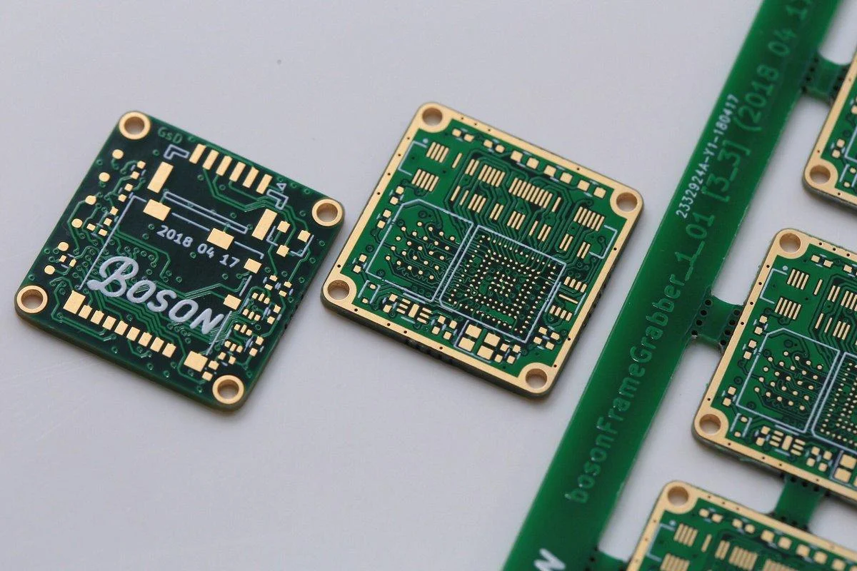
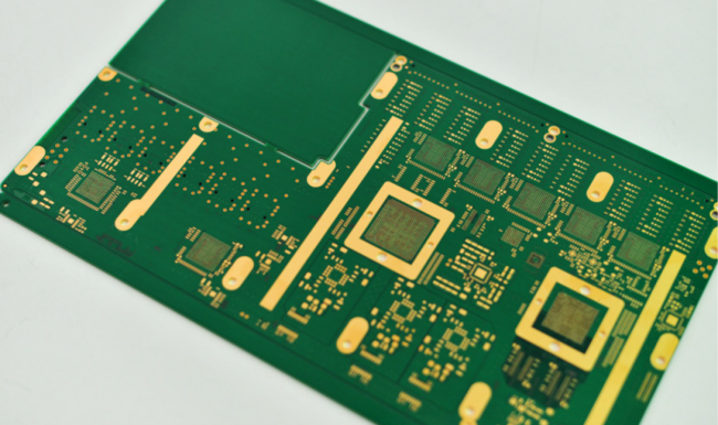
PCB manufactured by JLCPCB
Advantages:
The ENIG process provides excellent soldering performance and reliable characteristics. Its gold layer provides protection from humidity and ensures reliable connections.
It offers high corrosion resistance, protecting the PCB surface from oxidation and corrosion.
High contributes to maintaining good reflow performance.
It has good reliability and is suitable for many application scenarios, especially in high-demand electronic products.
Disadvantages:
Higher cost: The immersion gold process is more expensive compared to other surface treatment methods, primarily due to the high cost of gold as a material.
Environmental impact: The chemicals involved in the immersion gold process must be handled and disposed of properly to minimize their environmental impact. It’s not suitable for high-temperature applications: The immersion gold process may lead to embrittlement of the gold layer or peeling of the gold layer from the substrate under high-temperature conditions.
Not suitable for infrared welding due to the thicker immersion gold layer.
OSP (Organic Solderability Preservatives):
The organic protective film process involves coating the PCB copper surface with a layer of organic compounds. During the soldering process, this protective film can be removed to expose the fresh copper surface. This process is environmentally friendly and cost-effective, but the protective film has limited heat resistance and shelf life.
Advantage:
Suitable for Flexible Electronics: OSP is suitable for flexible electronic applications because it provides sufficient protection without adding to the rigidity of the board.
Relatively low cost: Some precious metal surface treatment methods, such as the immersion gold process, are more cost-effective due to the use of organic materials.
Suitable for short-term storage: This method is effective for short-term storage because it provides ample protection without compromising quality over a brief period.
Disadvantages:
Not suitable for long-term storage: The protective effect of OSP may diminish over time, making it unsuitable for applications requiring extended storage.
Sensitive to Ambient Humidity: The performance of OSP may be affected by ambient humidity, and high-humidity environments may lead to oxidation issues.
Not suitable for high reliability requirements: OSP may not be suitable for applications that demand high reliability and long-term stability, unlike some other surface treatment methods like immersion gold technology.
Immersion Silver :
The immersion silver process deposits a layer of silver directly onto the PCB surface, providing a smooth surface similar to ENIG but at a lower cost. However, the silver layer easily oxidizes in the air, so it requires proper packaging and quick use.
Advantages: It has good electrical conductivity and solderability, making it suitable for lead-free soldering. Additionally, it has a flat surface, making it suitable for high-frequency applications.
Disadvantages: The material is prone to vulcanization, which can affect conductivity. Care must be taken during storage and operation to avoid contamination and scratches.
Immersion Tin
The immersion tin process deposits a layer of pure tin on the PCB surface, which enhances solderability. However, the tin layer readily interacts with copper to produce tin whiskers, which can result in short circuits.
Advantages: Good solderability, lead-free process, and a flat surface suitable for fine-pitch components.
Disadvantages: Easily oxidized; sensitive to environmental conditions and requiring proper storage; the coating may develop whiskers after long-term storage.
Hard Gold Plating:
Hard gold plating is mainly utilized on edge connectors to offer outstanding wear resistance and electrical conductivity. This process is more costly and is typically only utilized for interfaces that necessitate frequent plugging and unplugging.
Advantage:
Good wear resistance makes it suitable for applications requiring wear resistance, such as gold fingers.
Good electrical conductivity. Hard gold plating can provide excellent electrical conductivity and ensure high-quality signal transmission.
Disadvantages:
high cost; not suitable for treating the entire board surface, only suitable for partial gold plating.
How to Choose a PCB Surface Finish
There are several factors to consider when selecting a PCB surface finsh:
Cost:
Cost is one of the primary factors to consider. For example, the ENIG process offers superior performance but comes with a higher cost, while OSP has a lower cost but offers more limited performance.
Application Fields: Certain applications have unique surface finish. For instance, high-frequency applications may opt for silver plating, while connectors that need wear resistance may opt for hard gold.
Solderability
Good solderability is essential for high-quality electronic assembly. HASL and ENIG generally provide the best solderability.
Environmental requirements:
Lead-free processes, such as lead-free HASL and ENIG, are compliant with RoHS regulations and are environmentally friendly choices.
Storage Period:
If the PCB needs to be stored for an extended period, it is advisable to select a surface treatment process with a long storage lifespan, such as ENIG or immersion silver.
Interfaces that are frequently plugged and unplugged:
For interfaces that require frequent plugging and unplugging, hard gold plating is the optimal choice due to its exceptional wear resistance.
Signal Integrity:
For high-speed or high-frequency applications, where surface flatness and minimization of signal loss are crucial, immersion gold and immersion silver may be a better choice.
In summary, the selection of a PCB surface treatment process depends on various factors, such as cost, performance requirements, environmental standards, storage life, and specific application requirements. JLCPCB offers a variety of surface treatment methods, including HASL, Lead-Free HASL, ENIG, and OSP. Electronic engineers must select the most suitable surface finish process based on specific application scenarios and budget to ensure the performance and reliability of PCB products. reliability
Post a Comment for "Exploring PCB Surface Finish A Comprehensive Guide"
Dont use outgoing links!