Common problems and solutions in PCB design
Printed circuit board (PCB) is an essential component of modern electronic equipment. During the PCB design process, designers often encounter various issues and problems, related but not limited to, layout inefficiencies, signal integrity concerns, and thermal management challenges. This article will explore common issues in PCB design and offer solutions to help engineers effectively address these challenges.
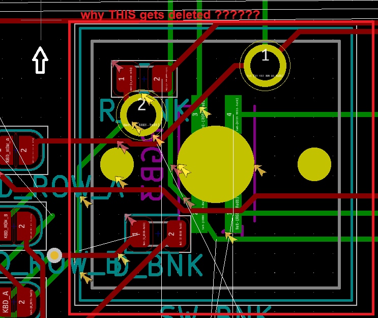
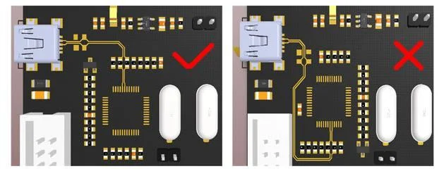
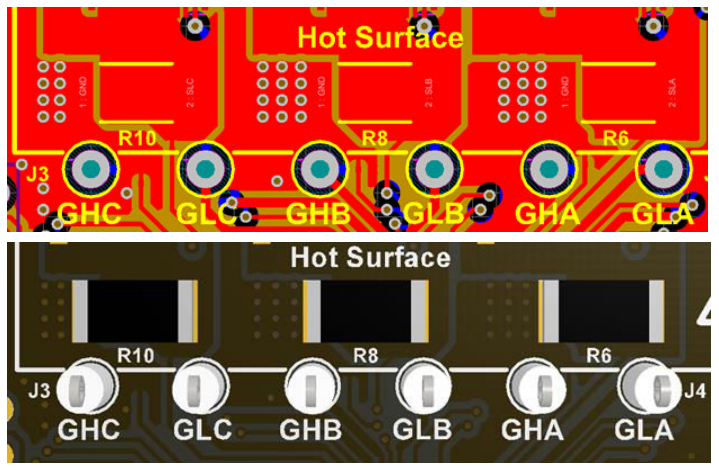
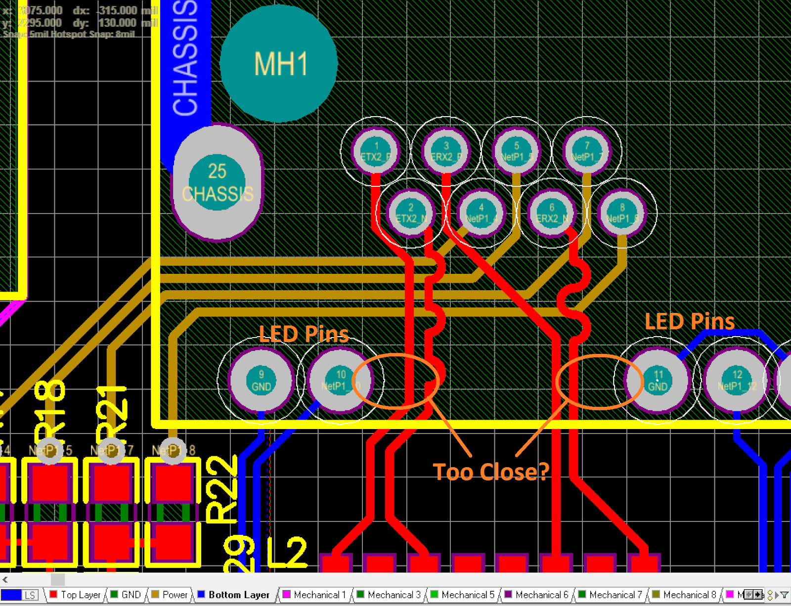
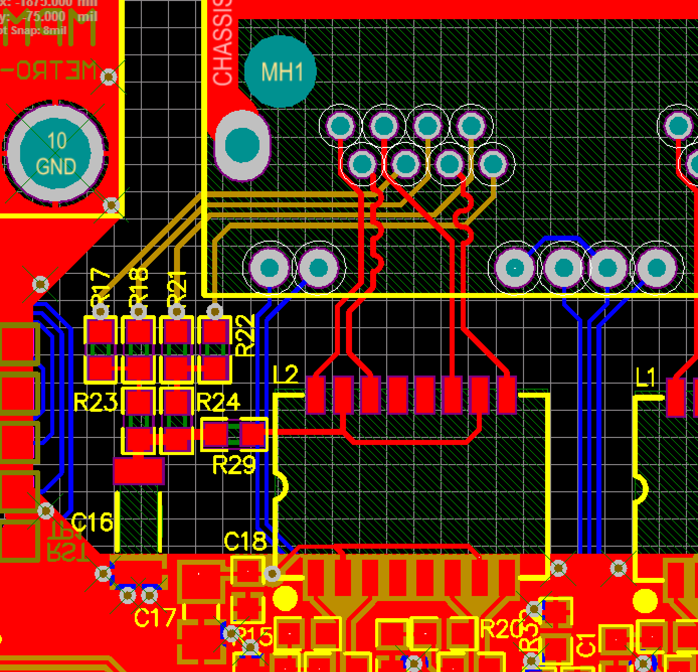
Unreasonable circuit layout
Circuit layout is crucial for maintaining signal integrity and electromagnetic compatibility. Unreasonable layout can lead to issues such as signal crosstalk and electromagnetic interference.
Solution:
1. Reasonably plan the hierarchy of the circuit board and separate high-speed signals from low-speed signals to minimize signal interference.
2. Divide the ground plane to prevent the formation of large-area ground plane loops and reduce electromagnetic interference.
3. Shorten the signal line as much as possible to minimize transmission delay and signal attenuation.
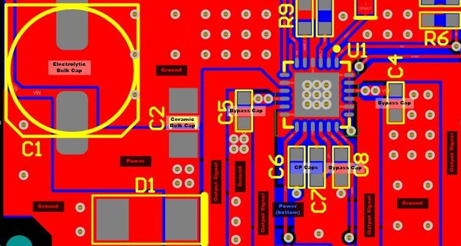
Power supply noise interference
Power supply noise may degrade circuit performance or even cause malfunction.
Solution:
1. Implement filter capacitors to eliminate power supply noise.
2. Add decoupling capacitors to the power supply to ensure stable power for each device.
3. Optimize the layout of the ground wire to ensure a solid ground wire reference plane and minimize noise resulting from the return flow of the ground wire.
Signal integrity issues
In high-speed signal transmission, maintaining signal integrity is a common challenge.
Solution:
1. Use the appropriate signal line width and spacing to ensure impedance matching and signal integrity.
2. Strengthen the ground reference plane of the signal layer to minimize the signal return path.
3. Implement terminal resistors and signal attenuators to minimize signal reflection and crosstalk.
Thermal management issues
High-power devices can lead to thermal issues, such as overheating and temperature unevenness.
Solution:
1. It is important to strategically design heat dissipation components, such as heat sinks and heat dissipation holes, to enhance heat dissipation efficiency.
2. Enhance heat dissipation by increasing the heat dissipation area to improve its ability.
3. Utilize a cooling pad to enhance the thermal contact between the device and the heat sink.
EMI/EMC issues
Electromagnetic interference and electromagnetic compatibility issues can lead to degradation in system performance. Solution:
1. Reasonably lay out the ground wire to minimize the return path and loop area.
2. Utilize a shielding cover to minimize electromagnetic radiation and electromagnetic interference from sensitive devices.
3. Apply a filter to eliminate high-frequency noise and interference.
Component selection issues
Using incorrect components may lead to unstable or unreliable circuit performance.
Solution:
1. Select the appropriate components and evaluate them based on design requirements and performance indicators.
2. Consider the temperature characteristics of the components to ensure that they operate normally within the specified temperature range.
3. Consider the reliability of components and select reliable brands and models.
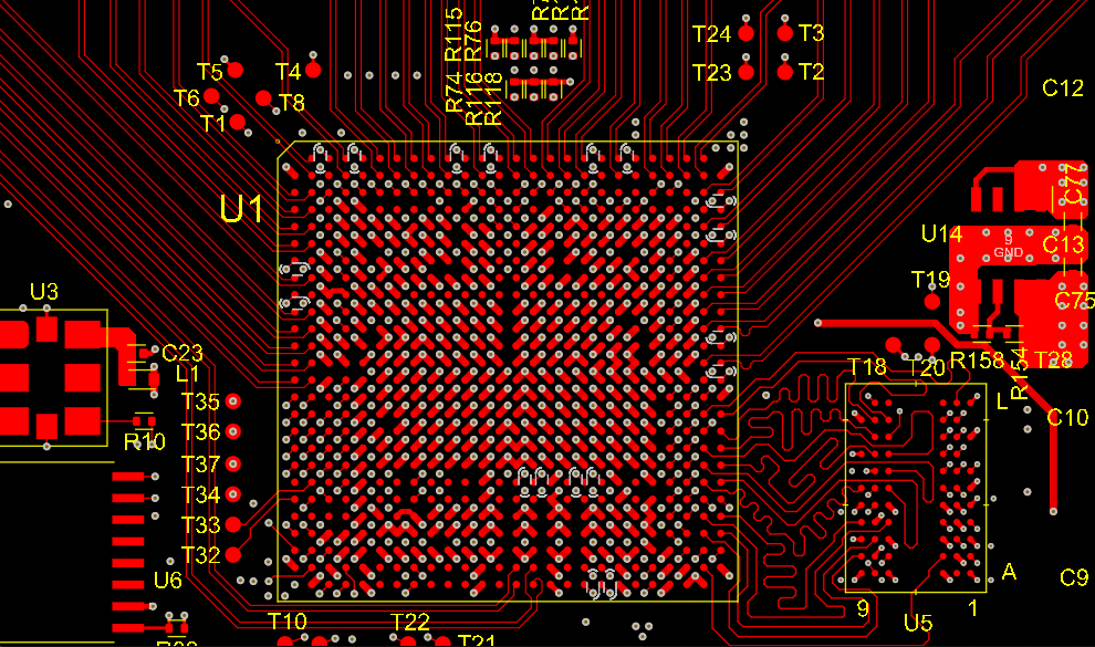
PCB size limitations
Limitations on PCB size can result in layout challenges or signal integrity issues.
Solution:
Plan the layout reasonably, taking into account size restrictions when planning the device layout and signal line direction.
2. Use multi-layer boards to incorporate additional wiring layers and ground planes in order to enhance signal integrity and electromagnetic compatibility.
3. Optimize the signal line direction, minimize the length of the signal line, and reduce delay and interference as much as possible.
Selecting a Package
In PCB design, choosing the appropriate package is crucial as it directly impacts the layout, connection method, and reliability of components.
Solution:
1. Understand the functions and usage environment of the components, and choose the appropriate packaging type based on the design requirements, such as SMD, THT, BGA, etc.
2. Refer to the component data sheet or the supplier's recommended packaging to ensure that the selection meets the electrical and mechanical specifications.
3. Customized Packaging: If there is no standard package that meets the requirements, you can consider creating a custom package. This requires accurate dimensions and pin layout, as well as appropriate materials and processing techniques.
4. Utilize 3D modeling tools to validate the packaging, identify potential collisions between the package and other components, and guarantee the precision and assembly of the package.
Manufacturing and assembly issues
Issues that may arise during the manufacturing and assembly process include inadequate welding, component misalignment, and so on.
Solution:
Select the appropriate manufacturer to guarantee manufacturing quality and process reliability.
Conduct thorough prototype testing to verify the manufacturability and ease of assembly of the design.
Optimize the reflow process by using the appropriate reflow temperature and flux to enhance welding quality.

JLCPCB : $2 for 1~8 Layer PCBs ,60 coupons for new customers !
PCB Prototype + Assembly from $2!
Conclusion :
During the PCB design process, it is inevitable to encounter various challenges. By employing hierarchical planning, rational layout, appropriate power and signal processing techniques, and effective thermal management, engineers can effectively address these issues and enhance the quality and performance of PCB designs.
Post a Comment for " Common problems and solutions in PCB design"
Dont use outgoing links!