Fullbridge Class-D Amplifier Project in SMD Mini Ultra Powerful
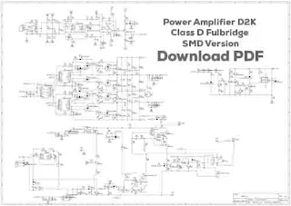
Hello, friends in this post I will make a Class-D Fullbirdge D2K project designed by Mr. Kartino S. which I will design the PCB using SMD components, but not all of them use SMD components, some components still use through-hole or DIP components. Let's look at the scheme of the Classbridge D-D2K Fullbridge power amplifier below.
 |
| Download PDF |
The input balance circuit that uses a dual op-amp IC. I use the MC33078 low noise op-amp. Then the comparator uses TL071 IC, Level shifter uses Transistor 2n5401. For the IC logic it uses CD4049, then the MOSFET driver uses IR2110 IC, for the totem-pole I use Transistor BD139.140.
For MOSFETs and Low Pass filter circuits like this. I will explain more in detail after the PCB is there and begin to be assembled.
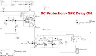
For features, I added DC Protection, which functions to disconnect the speaker relay if the output exceeds DC More than 3V.
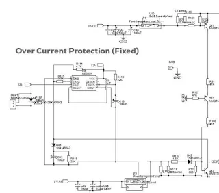
Then there are signal indicators, clips, protection, and On. I also added this OCP or Over Current Protection, which functions to turn off the PWM signal and disconnect the speaker relay if there is an overload. and OCP I made fixed.
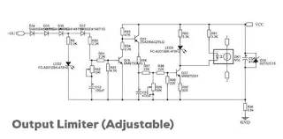
I also added an LED + LDR limiter whose sensor is from the amplifier's output clip signal itself, so this circuit to put the limit on the output before the clip occurs. So, making this amplifier will rarely clip even at all, depending on the settings desired. Because this limiter has settings, it can set a maximum output as desired, for example, only want to come out 100W RMS can. For the settings later I will explain in another post.
I have designed this PCB layout before, oh yes I am using the easyeda.com application, if you want to try this project I will share the link : D2K Fullbridge SMD Project work
The dimensions of this PCB are 10x18.6 cm. mini enough for the size of a full-bridge class-d amplifier. mini dimension because using some SMD components, I choose SMD components in certain parts, the part where the components are only passed by small currents and through-hole for currents and large power dissipation so that the amplifier can work as much as possible.
Maybe some of your friends will feel inferior to soldering the SMD component, because the components are small and certainly more difficult to solder than DIP components or through holes. So don't worry, you can buy PCBs and all of the SMD components are soldered together, namely by using the SMT Assembly, PCB and SMT Assembly services that I use, namely at JLCPCB, com. also quite affordable, we can save time and energy to solder SMD components.


Здравствуйте. Вы обещали сделать отдельный пост о настройке усилителя. Какие значения сопротивление необходимо выставить на подстроечных резисторах?
ReplyDeleteWhich trimming resistor do you mean?
DeleteМеня интересует значение сопротивления на R82, R89 и на R35 уже на настроенном усилителе. И за что конкретно отвечает каждое из этих сопротивлений?
DeleteSee at easyeda
DeleteДа я знаю номинальное значение, но я не могу настроить. Дайте пожалуйста ваши значения после настройки или запишите видео на канале, как настроить лимит и клип? Как настроить ограничения по току и т.д как настроить эти резисторы
Delete